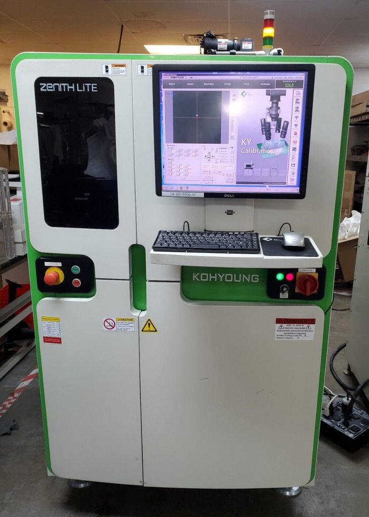
What is 3D Automatic Optical Inspection Machine?
Introduction
A 3D Automatic Optical Inspection (AOI) Machine is an advanced device used in the electronics manufacturing industry to perform precise inspection of printed circuit boards (PCBs) and other components. These machines utilize optical imaging and sophisticated algorithms to detect defects in electronic assemblies, ensuring quality control and compliance with design specifications.
Working Principles
The fundamental working principle of a 3D AOI machine revolves around capturing high-resolution images of the PCB and analyzing these images to identify defects. This process can be broken down into several key stages:
1. Image Acquisition
3D AOI machines use a combination of cameras, lighting, and optical sensors to capture detailed images of the PCB. The setup typically includes:
- Multiple Cameras: High-resolution cameras are positioned at various angles to capture different views of the PCB. These cameras can be both top-down and angled to get a complete view of the components.
- Structured Light Projectors: These projectors emit patterns of light (often in the form of stripes or grids) onto the PCB surface. The deformation of these patterns when projected on the PCB is used to calculate the 3D shape and dimensions of the components.
- Coherent Illumination: Different lighting techniques, such as ring lights, side lighting, and coaxial lighting, are used to enhance the visibility of specific features and defects.
2. 3D Image Reconstruction
The captured images are processed to reconstruct a 3D model of the PCB. This involves:
- Triangulation: By analyzing the deformation of the projected light patterns, the system can calculate the height and shape of the components on the PCB. Triangulation algorithms are used to correlate the images from different cameras and generate a precise 3D model.
- Surface Mapping: The system maps the surface topology of the PCB, identifying the exact location, orientation, and height of each component.
3. Defect Detection
With the 3D model of the PCB, the AOI machine performs a detailed inspection to detect various types of defects. The common defects that 3D AOI machines are designed to detect include:
- Solder Joint Defects: These include insufficient solder, excessive solder, solder bridges, and solder voids. The 3D AOI machine can measure the volume and shape of the solder joints to ensure they meet the required specifications.
- Component Placement Issues: Misaligned, missing, or skewed components are identified by comparing the actual placement with the expected position.
- Coplanarity Issues: For components with multiple leads, such as QFPs and BGAs, the machine checks if all leads are properly seated and coplanar with the PCB surface.
- Surface Defects: Scratches, contaminants, and other surface imperfections are detected by analyzing the surface texture and reflectivity.
4. Algorithm and Software Integration
The heart of the 3D AOI machine is its software, which uses advanced algorithms to analyze the 3D data. Key aspects of the software include:
- Pattern Recognition: Machine learning and pattern recognition techniques are employed to identify and classify defects. The system is trained using a large dataset of defect images, allowing it to recognize even subtle deviations from the norm.
- Threshold Settings: Users can configure the inspection thresholds to specify the acceptable limits for various parameters, such as component height, solder volume, and placement accuracy.
- Real-time Analysis: Modern 3D AOI machines are capable of real-time analysis, providing instant feedback on the inspection results. This enables immediate corrective actions to be taken, reducing the likelihood of defective products reaching the market.
Advantages of 3D AOI Machines
The use of 3D AOI machines offers several advantages over traditional 2D inspection methods:
- Enhanced Accuracy: The ability to measure height and volume in addition to the X and Y dimensions allows for more precise defect detection.
- Comprehensive Coverage: 3D AOI machines can inspect complex components and densely packed PCBs more effectively than 2D systems.
- Reduced False Alarms: By providing a complete 3D profile of the PCB, these machines reduce the likelihood of false positives, as the inspection is based on more comprehensive data.
- Process Optimization: The detailed inspection data can be used to optimize the manufacturing process, identifying trends and areas for improvement.
Applications
3D AOI machines are widely used in various stages of the electronics manufacturing process, including:
- Post-Soldering Inspection: After soldering, the AOI machine checks the quality of solder joints and component placement.
- Final Quality Control: Before final assembly and packaging, the AOI machine performs a thorough inspection to ensure that the product meets all quality standards.
- In-Line Inspection: Integrated into the production line, 3D AOI machines provide continuous monitoring and feedback, enabling real-time adjustments to the manufacturing process.
Conclusion
3D Automatic Optical Inspection machines represent a significant advancement in the field of electronic manufacturing quality control. By leveraging advanced imaging techniques and sophisticated algorithms, these machines provide precise, reliable, and comprehensive inspection capabilities, ensuring the highest quality standards for electronic assemblies. Their ability to detect a wide range of defects in real-time makes them an invaluable tool for modern electronics manufacturing.


